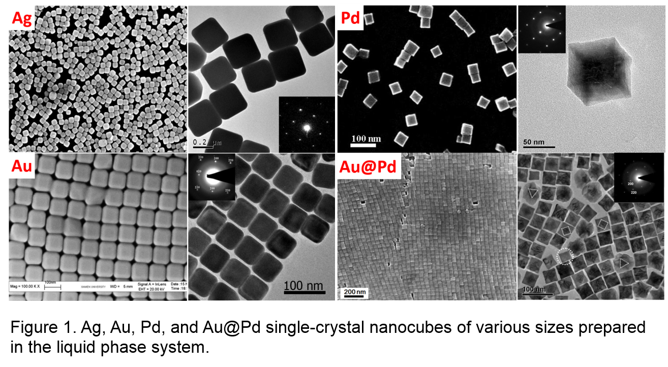
Monodisperse Single-crystal Metal Nanocubes
Metal nanocrystals with special shapes have attracted steadily growing interest due to unique properties and intriguing applications. In most of their potential applications, the quality and the structure of the surface of nanocrystals will undoubtedly play a very important role in determining their functions. Surface-enhanced Raman scattering (SERS) with its high surface sensitivity becomes a powerful technique in studying the optical property of metal nanocystals. Usually, the SERS activity strongly depends on the styles and shapes of metal nanocystals. In the past years, SERS substrate usually is the rough surface, which is difficult to develop the theoretical model based on the experimental data obtained from the ill-defined surfaces because of the heterogeneity in the surface structure. To cope with this difficulty, it is worthwhile to construct the atomic-scale well-defined nanostructure surface which has well-controlled shape, size and space between each other.
Recently, Our group have developed some simple methods in liquid-phase for synthesizing monodisperse single-crystalline Pd, Au, Ag and Au@Pd nanocubes. Noble metal nanocubes exhibit high SERS activity, which are explained by a theoretical calculation using three-dimensional finite difference time domain (FDTD) method. The size- and shape-controlled nanocrystals may be a promising material to bridge the gap between highly rough and single crystal surfaces, and hence allows us to obtain a deep insight into the SERS mechanism and make a mighty advance on understanding and application of nanocrystals.
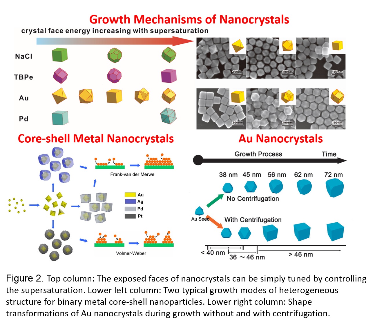
Growth Mechanisms of Nanocrystals
To extend the shape-controlled growth of nanocrystals, it is highly desirable to develop new synthesis methods and get the deep insight of the growth mechanism. We propose that the exposed crystal faces can be simply tuned by controlling the supersaturation, and higher supersaturation will result in the formation of crystallites with higher surface-energy faces. We have successfully applied it for the growth of ionic (NaCl), molecular (TBPe), and metallic (Au, Pd) micro/nanocrystals with high-surface-energy faces. The above proposed strategy can be rationally designed to synthesize micro/nanocrystals with specific crystal faces and functionality toward specific applications.
Based on the systematic study on the heterogeneous growth mechanism, we have preliminarily proposed a general rule that the atomic radius, bond dissociation energy, and electronegativity of the core and shell metals play key roles in determining the conformal epitaxial layered growth mode. This rule would be help for designing and fabricating more complex nanostructures, such as multiple-shell nanostructures and metal-semiconductor nanocomposites.
The growth of nanoparticles will be affected by the external environment, we found that without centrifugation the Au nanooctahedron seeds grew into truncated octahedrons cuboctahedrons, nanocubes truncated along the [111] and [110] directions, and slightly truncated nanocubes. The mass transfer of Au monomers can be accelerated and the surface reaction step then plays a critical role in shape evolution.
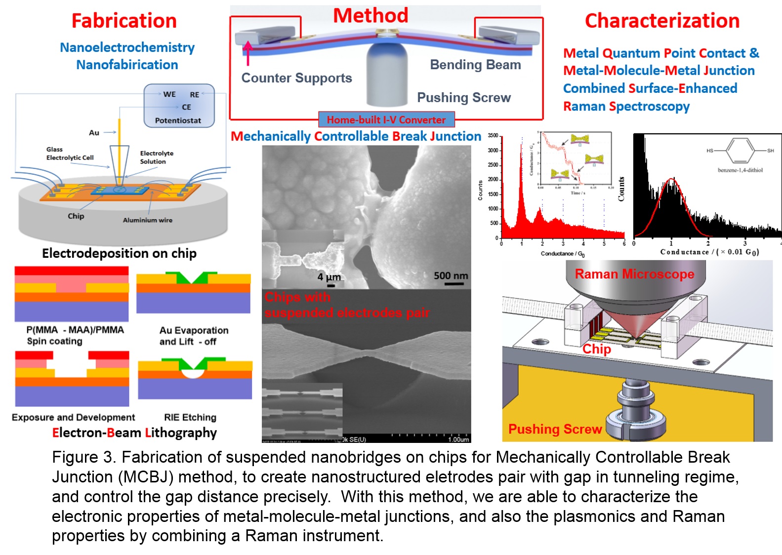
Fabrication of Nanostructures by MEMS method
Nanostructures with gaps in tunneling regime exhibit great research interests because of their widely application in nano-electronics and molecular electronics, and their unique properties in plamonics and catalysis. Mechanically Controllable Break Junction (MCBJ) is an excellent technology to create gap and control the gap distance in tunneling regime precisely and in-situ.
Our group has developed two approaches for the MCBJ method. By using the Microelectromechanical Systems (MEMS) technologies, we firstly fabricate microelectrodes pairs on silicon chips. One of our approach is combining nanoelectrochemistry to electrodeposit interested metals to make the microelectrodes pair form suspended nano-restriction contact. The other one is using Electron-Beam Lithography to fabricate suspended nano-bridge on microelectrodes pair. By bending the chips using a pushing screw underneath, the nanostructures will be broken into nano-electrodes pairs with gaps. With a large reduction ratio, the screw’s sub-micrometer pushing makes gap separation sub-angstrom changes, which means the gap can be controlled precisely in tunneling regime.
The electrodes pair created by MCBJ can be stable, and the break and junction process can be repeated over ten thousands times, whilst the gap can be easily tuned to fit the target molecule length. Thus it is useful to fabricate and measure the electronic properties of Metal Quantum Point Contacts (MQPCs) and Metal-Molecule-Metal (MMM) junctions
As nanostructures show Surface Plasmonic Resonance (SPR) under visible laser illumination. There exists great enhanced electromagnetic field between the gap of nanostructures. By combining Surface-Enhanced Raman Scattering (SERS) technology, we are able to characterize the Raman and electronic properties of molecular junction simultaneously. Besides, as the laser provide a forceful stimuli, the molecular junction in the tunneling regime might also exhibit extraordinary phenomena. By the MCBJ method, the gap distance can be precisely controlled, which can be helpful to measure the nanostructure scattering in-situ, and investigate the relationship between SPR and SERS, even by applying the bias. On the same time, in order to stabilize the molecular junction and eliminate the influence of impurities, and do some low-temperature or temperature-adjustable experiments, we have designed and fabricate a Low-Temperature Ultra-High-Vacuum MCBJ-SERS combined system (LT-UHV-MCBJ-SERS).
References
1. Liu, B.; Xiang, J.; Tian, J.-H.; Zhong, C.; Mao, B.-W.; Yang, F.-Z.; Chen, Z.-B.; Wu, S.-T.; Tian, Z.-Q. Controllable nanogap fabrication on microchip by chronopotentiometry. Electrochimica Acta 50, 3041-3047 (2005).
2. Xiang, J.; Liu, B.; Wu, S. T.; Ren, B.; Yang, F. Z.; Mao, B. W.; Chow, Y. L.; Tian, Z. Q. A Controllable Electrochemical Fabrication of Metallic Electrodes with a Nanometer/Angstrom-Sized Gap Using an Electric Double Layer as Feedback. Angew. Chem. Inter. Edit. 44, 1265-1268 (2005).
3. Tian, J. H.; Liu, B.; Li, X.; Yang, Z. L.; Ren, B.; Wu, S. T.; Tao, N.; Tian, Z. Q. Study of Molecular Junctions with a Combined Surface-Enhanced Raman and Mechanically Controllable Break Junction Method. J. Am. Chem. Soc. 128, 14748-14749 (2006).
4. Tian, J. H.; Yang, Y.; Bo, L.; Schöllhorn, B.; Wu, D. Y.; Maisonhaute, E.; Muns, A. S.; Chen, Y.; Amatore, C.; Tao, N.; Tian, Z. Q. The fabrication and characterization of adjustable nanogaps between gold electrodes on chip for electrical measurement of single molecules. Nanotech. 21, 274012 (2010).
5. Tian, J. H.; Yang, Y.; Zhou, X. S.; Schöllhorn, B.; Maisonhaute, E.; Chen, Z. B.; Yang, F. Z.; Chen, Y.; Amatore, C.; Mao, B. W.; Tian, Z. Q. Electrochemically Assisted Fabrication of Metal Atomic Wires and Molecular Junctions by MCBJ and STM-BJ Methods. ChemPhysChem 11, 2745-2755 (2010).
6. Yang, Y.; Liu, J. Y.; Chen, Z. B.; Tian, J. H.; Jin, X.; Liu, B.; Li, X.; Luo, Z. Z.; Lu, M.; Yang, F. Z.; Tao, N.; Tian, Z. Q. Conductance histogram evolution of an EC–MCBJ fabricated Au atomic point contact. Nanotechnology 22, 275313 (2011).
7. Yang, Y.; Chen, Z. B.; Liu, J. Y.; Lu, M.; Yang, D. Z.; Yang, F. Z.; Tian, Z. Q. An electrochemically assisted mechanically controllable break junction approach for single molecule junction conductance measurements. Nano Research 4, 1199-1207 (2011).