Introduction
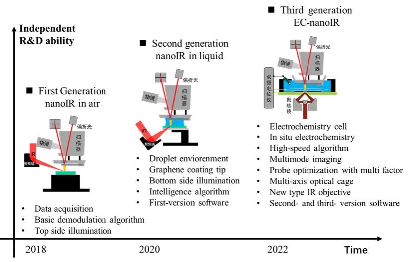
Infrared nanospectroscopy (nanoIR) has attracted broad attention since 2013. Early nanoIR systems, however, struggled to analyze samples in aqueous environments because water strongly absorbs infrared light and damps the oscillation of AFM probes. Characterizing samples in liquids, particularly at electrochemical interfaces, has therefore remained a long-standing challenge.
With support from a national scientific-instrumentation program, our team developed an advanced liquid-environment nanoIR platform over the past five years. We studied its underlying physical principles, measurement and control technologies, environmental control, and sample-preparation methods. These efforts led to three generations of nanoIR systems that progressively addressed key technical challenges.
The first-generation system established the technical foundation, including software, hardware, data acquisition, and online algorithms. The second generation introduced a bottom-excitation module and enabled nanoIR experiments in aqueous environments. The current third-generation system uses a customized electrochemical cell to detect in situ nanoIR signals from electrochemical reactions at solid/liquid interfaces for the first time. It also enables nanoscale multimodal imaging that correlates morphology, mechanics, electrical information, and chemical signatures.
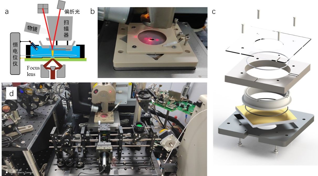
The third-generation nanoIR system is built around a customized spectroelectrochemical cell. The cell consists of a BaF2 substrate coated with a 10 nm gold film as the working electrode and is illuminated directly from the bottom through a reflective objective. The cell is mounted on a three-axis nanopositioning stage and integrated into a multi-axis cage system for stability and compatibility.
To support the system, we developed integrated measurement and control software covering mid-IR laser control, AFM operation, electrochemical functions, and data processing. The software includes algorithms for optimizing IR pulse excitation and transmitting nanoIR signals to the AFM controller for simultaneous display with correlated morphology. The nanopositioning stage enables sample scanning and can be combined with intelligent algorithms for high-speed nanoscale infrared hyperspectral imaging.
Performance
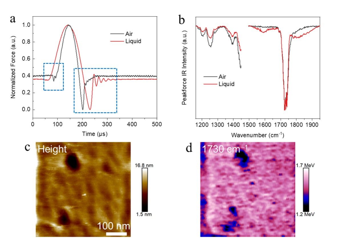
Polymethyl methacrylate (PMMA), polycarbonate (PC), polystyrene (PS), and PMMA-b-PS block-copolymer films are suitable benchmark samples for nanoIR characterization. AFM force curves measured on PMMA films show clear differences between air and aqueous environments: the free oscillation amplitude of the probe persists in air but decreases rapidly in solution, and the jump-to-contact point is much more pronounced in air.
The nanoIR spectra maintain a good signal-to-noise ratio in both air and solution, although the baseline is higher in solution. By imaging the C=O bond distribution at a fixed excitation wavenumber of 1730 cm-1, we demonstrated stable high-performance nanoIR microscopy in aqueous environments. Correlated nanoscale imaging of morphology and chemical information revealed a heterogeneous C=O distribution and verified the effectiveness of the system.
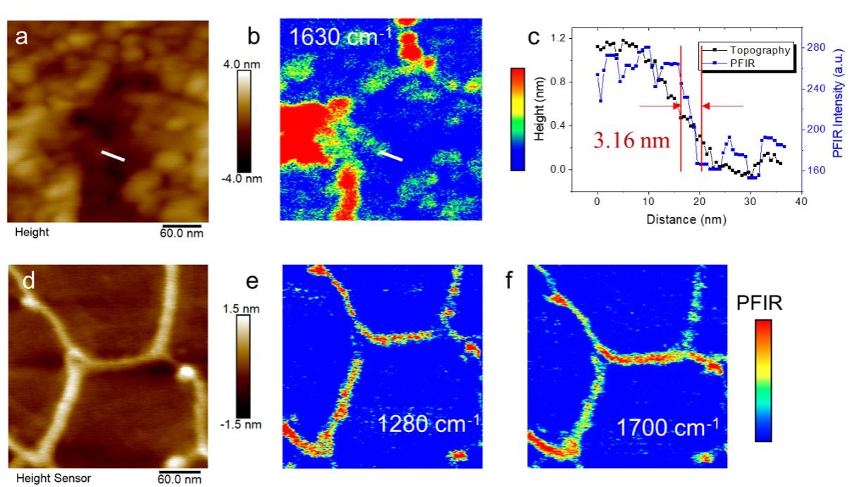
To demonstrate sensitivity, we prepared ultrathin samples on an ultrathin gold-film substrate using the Langmuir-Blodgett (LB) method. AFM topography and nanoIR images at 1630 cm-1 showed strong correlation. Comparing the topography profile with the nanoIR intensity indicated a spatial resolution of 3.16 nm perpendicular to the edge of the LB film, exceeding the previously reported 6 nm resolution. We also imaged DNA double-helix chains at 1280 and 1700 cm-1, observing helix-like structures at DNA-strand edges and demonstrating high sensitivity on a 1.2 nm thick sample.
In Situ NanoIR Spectroscopic Observation of Electrochemical Processes
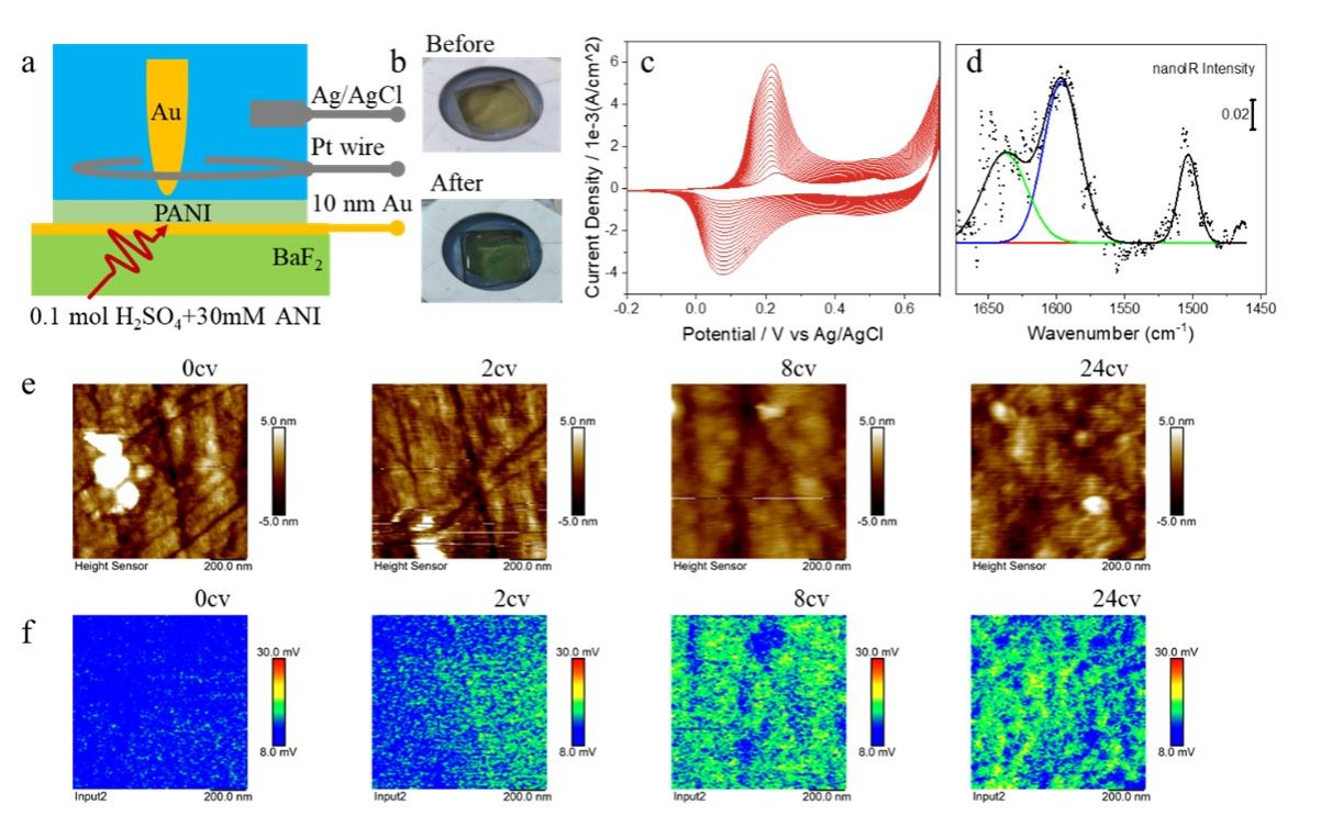
We demonstrated in situ electrochemical measurements with the third-generation nanoIR system by monitoring aniline electropolymerization. The infrared beam passed through a BaF2 substrate to reach the probe-sample nanogap. The reaction was carried out in an electrochemical cell containing 0.1 M H2SO4 and 30 mM aniline.
During polymerization, the reaction area at the electrode interface changed color from light yellow, reflected by the 10 nm gold film, to dark green polyaniline. Cyclic voltammetry showed shifts and increases in the first oxidation and reduction peaks of aniline over multiple cycles, indicating polymerization and electrochemical proton doping. Infrared spectra of the film after reaction showed three main peaks associated with benzene-ring and quinone structures. When the IR wavenumber was fixed at 1500 cm-1, the vibrational signal of the benzene-ring skeleton became stronger during the reaction and showed a heterogeneous distribution correlated with morphology.