
Plasmonics
Conduction electrons in metal or metal-like nanomaterials can be coherently excited by incident light to collectively oscillate at metal/dielectric interfaces. The collective oscillating mode of electrons and the nanomaterials that support are referred to as surface plasmons and plasmonic materials, respectively. There are two types of surface plasmons: (i) localized surface plasmons (LSP), in which coherent electrons oscillate around the NP surfaces or nanoscale crevices, and (ii) propagating surface plasmons (that is, surface plasmon polaritons (SPPs)), in which the coherent electrons oscillate as a longitudinal wave at extended metal surfaces. Nano-optics, especially the sub-field plasmonics is the study of light at nanoscale and the study of the interaction between light and nano-scale objects supporting surface plasmons.
Surface plasmons support the characteristic extinction energy and strong electromagnetic field in the vicinity of the nanostructures, as well as hot carriers and local heating during the relaxation of surface plasmons, which has great importance for a wide variety of applications ranging from biosensors, spectroscopies and microscopy, catalysis, optoelectronics and solar cells.
Our research interests in nano-optics and plasmonics are to rational design novel nano-devices for nano-spectroscopies, nano-sensor and nano-imaging based on the comprehensive understanding of the mechanism of plasmon-enhanced spectroscopies and its correlation to the plasmonic properties of nanostructures, by means of new theories, concepts and simulation methods. The relation of our plasmonic researches to other researches in our group could be described in Figure 1.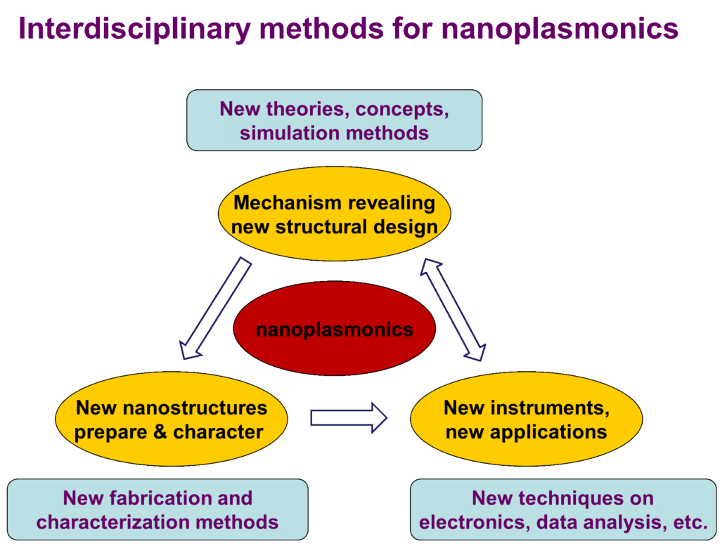
Plasmonic properties and SERS activity from transition metal nanostructures
1. SERS from transition-metal cauliflower-like structures prepared by electrochemical roughening methods
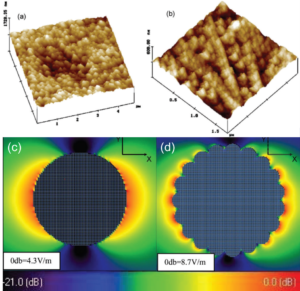
Figure 2. STM (a) and AFM (b) images of electrochemically roughened Pt and Rh electrodes, respectively. FDTD simulated electric field distribution for spherical (c) and cauliflower-like (d) Rh nanoparticles. The incident beam illuminates along the y direction with x-polarization[1].
2. SERS from gold@transition-metal core@shell nanostructures
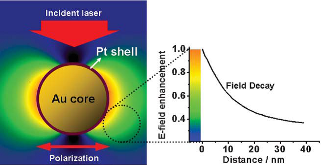
Figure 3. Schematic illustration of the electromagnetic field distribution around Au@Pt core–shell nanoparticles under laser irradiation (left). The dependence of the electromagnetic field strength (normalized with the strength on the Pt surface) on the distance from the Pt shell is shown in the right plot, indicating a substantially strong field enhancement can still be obtained on the surface[2].
Plasmonic properties of a hybrid structures including plasmonic nanoparticles on probing material surfaces
1. The first and second generations of hotspots
The first generation of hotspots were generated from single nanostructures such as nanospheres and nanocubes (FIG. 4a,b), or nanorods freely suspended in a homogeneous medium. These hotspots exhibit moderate SERS-activity; however, some rationally designed single nanoparticles with sharp corners and/or with intra-particle gaps, such as Au and Ag nanostars, nanoflowers and mesocages exhibit much higher SERS-activity.
The second generation of SERS hotspots are generated from coupled nanostructures with controllable inter-particle nanogaps (for example, the NP dimers shown in FIG. 4c,d or oligomers and NP arrays shown in Fig. 4e,f) or inter-unit nanogaps in nano-patterned surfaces (FIG. 4g,h). Such hotspots exhibit excellent SERS activity. Because the average SERS intensities from coupled plasmonic nanostructures are typically 2–4 orders of magnitude greater than that from single nanostructures, they are more commonly used for trace-molecule detection. SERS hotspots from coupled nanostructures are extremely small (1–5 nm), but the Raman signals of probe molecules at the hotspots contribute significantly to the total Raman signal.
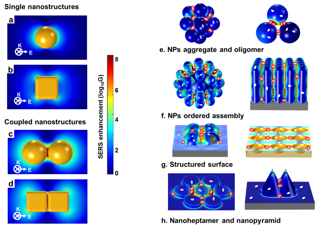
Figure 4. First- and second-generation SERS hotspots for trace-molecule detection.
2. The third-generation hotspots
In general, first- and second-generation hotspots are not well suited for surface analysis of many materials. For example, widely used materials such as silicon wafer or ceramics cannot be squeezed into the extremely tiny and narrow regions of the hotspots formed by coupled nanostructures, such as those shown in FIG. 4c-h. Therefore, it is highly desirable to design plasmonic nanostructures that can have hotspots right on the surface of the materials to be probed. The goal can be realized by taking into account of the effect of the materials to be probed in the design of the plasmonic nanostructures. Because, the localized SPR response and local EM field distribution not only depends on the shape, size of plasmonic nanostructures, but also depends sensitively on the dielectric properties of probe materials close to the plasmonic nanostructures. The hotspot generated from the hybrid structures consisting of plasmonic nanostructures and the probe materials can be considered third-generation hotspots. Representative examples of such hybrid structures are shown in FIG. 5.
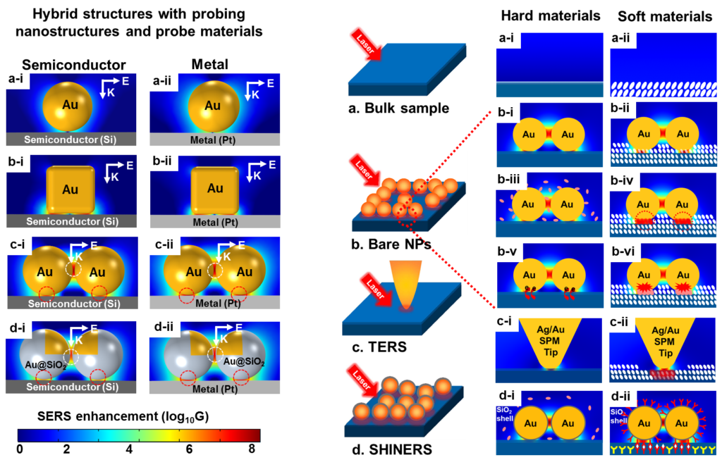
Figure 5. Third-generation SERS hotspots for surface analysis of materials.
3. The plasmonic nature of SHINERS from general materials
SHINERS is a representative technique supporting third-generation hotspots. The working principle of SHINERS for gold, silver, and more general metal single-crystal surfaces have been extensively studied in our group[4-8].
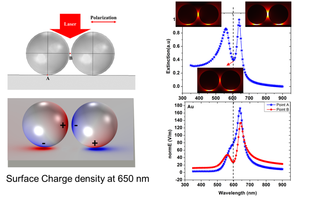
Figure 6. Fano Resonance nature of a Au@SiO2 nanoparticle dimer on a flat gold surface. Coupled dipole of Nanoparticles induce the imaginary dipole on the metal or dielectric surfaces, to form a magnetic-dipole-like mode. It is the plasmonic dark mode with less irradiative efficiency, but with strong near field.
References
1. Tian, Z.-Q. et al. Surface-enhanced raman scattering from transition metals with special surface morphology and nanoparticle shape. Faraday Discuss. 132, 159-170 (2006).
2. Tian, Z.-Q., Ren, B., Li, J.-F. & Yang, Z.-L. Expanding generality of surface-enhanced raman spectroscopy with borrowing sers activity strategy. Chem. Commun., 3514-3534 (2007).
3. Ding, S.-Y. et al. Nanostructure-based plasmon-enhanced raman spectroscopy for surface analysis of materials. Nature Reviews Materials 1, 16021 (2016).
4. Li, J.-F. et al. Extraordinary enhancement of raman scattering from pyridine on single crystal au and pt electrodes by shell-isolated au nanoparticles. J. Am. Chem. Soc. 133, 15922-15925 (2011).
5. Li, J.-F. et al. Shell-isolated nanoparticle-enhanced raman spectroscopy. Nature 464, 392-395 (2010).
6. Li, C.-Y. et al. “Smart” ag nanostructures for plasmon-enhanced spectroscopies. J. Am. Chem. Soc. 137, 13784-13787 (2015).
7. Li, J.-F., Anema, J.R., Wandlowski, T. & Tian, Z.-Q. Dielectric shell isolated and graphene shell isolated nanoparticle enhanced raman spectroscopies and their applications. Chem. Soc. Rev. (2015).
8. Ding, S.-Y., Yi, J., Li, J.-F. & Tian, Z.-Q. A theoretical and experimental approach to shell-isolated nanoparticle-enhanced raman spectroscopy of single-crystal electrodes. Surf. Sci. 631, 73-80 (2015).
9. Chen, S. How to Light Special Hot Spots in Multiparticle-Film Configurations. ACS Nano 10, 581-587 (2016).
Plasmon-mediated chemical reaction
Plasmon-mediated chemical reactions (PMCRs) are processes that make use of nanostructure-based surface plasmons as mediators to redistribute and convert photon energy in various time, space and energy scales, thereby driving chemical reactions by localizing photon, electronic and/or thermal energies. PMCRs can enhance the efficiency of an array of reactions, with potential advantages and unique features over thermochemistry, electrochemistry, photochemistry and photocatalysis.
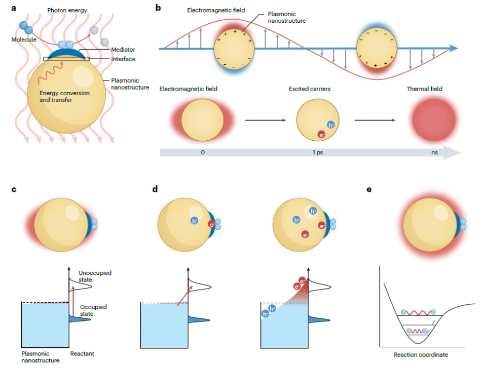
Figure 7. Plasmon-mediated chemical reactions and their main mechanism. a | Schematic of PMCRs. b | Excitation and relaxation of surface plasmons, as well as the corresponding three main effects, including the enhanced electromagnetic near field, excited carriers and local heating. A microscopic view of plasmon-mediated chemical reactions, namely, c | enhanced electromagnetic field mediated photochemical reactions, d | excited carriers mediated photocatalytic reactions from direct change transfer (left) to indirect charge transfer (right), and e | local heating mediated thermal reactions.
1. Disentangling charge carrier from photothermal effects
(1) A key question in this burgeoning field which has not, as yet, been fully resolved, relates to the precise mechanism through which the energy absorbed through plasmonic excitation, ultimately drives such reactions. Among the multiple processes proposed, two have risen to the forefront: plasmon-increased temperature and generation of energetic charge carriers. However, it is still a great challenge to confidently separate these two effects and quantify their relative contribution to chemical reactions. Here, we describe a strategy based on the construction of a plasmonic electrode coupled with photoelectrochemistry, to quantitatively disentangle increased temperature from energetic charge carriers effects. A clear separation of the two effects facilitates the rational design of plasmonic nanostructures for efficient photochemical applications and solar energy utilization.
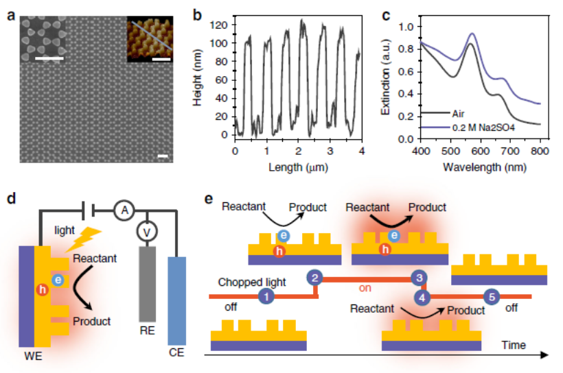
Figure 8. Structures of the as-prepared plasmonic electrode and photoelectrochemical system.
(2) Surface plasmons (SPs) are able to promote chemical reactions through the participation of the energetic charge carriers produced following plasmons decay. Using p-aminothiophenol (PATP) as a probe molecule, we used surface-enhanced Raman spectroscopy to follow the progress of its transformation, in situ, to investigate systematically the role of hot electrons and holes. The energetic carrier mediated PATP oxidation was found to occur even in the absence of oxygen, and was greatly influenced by the interface region near the gold surface. The observed reaction, which occurred efficiently on Au@TiO2 nanostructures, did not happen on bare gold nanoparticles (NPs) or core−shell nanostructures when a silicon oxide layer blocked access to the gold. Moreover, the product of the PATP oxidation with oxygen on Au@TiO2 nanostructures differed from what was obtained without oxygen, suggesting that the mechanism through which “hot holes” mediated the oxidation reaction was different from that operating with oxygen activated by hot electrons.
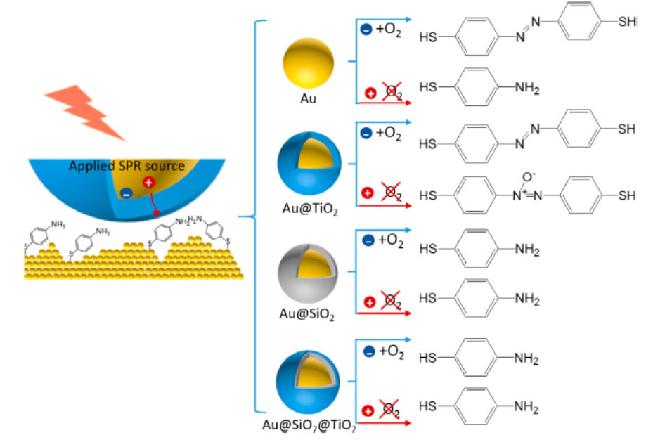
Figure 9. Schematic of the SPs-mediated PATP oxidation that is regulated by the interface between the SPs source and reactant.
2. Plasmonic catalysis to improve the efficiency and regulate the selectivity
(1) Plasmonic nanoreactors regulating selective oxidation by energetic electrons and nanoconfined thermal fields Optimizing product selectivity and conversion efficiency are primary goals in catalysis. However, efficiency and selectivity are often mutually antagonistic, so that high selectivity is accompanied by low efficiency and vice versa. Also, just increasing the temperature is very unlikely to change the reaction pathway. Here, by constructing hierarchical plasmonic nanoreactors, we show that nanoconfined thermal fields and energetic electrons, a combination of attributes that coexist almost uniquely in plasmonic nanostructures, can overcome the antagonism by regulating selectivity and promoting conversion rate concurrently. For propylene partial oxidation, they drive chemical reactions by not only regulating parallel reaction pathways to selectively produce acrolein but also reducing consecutive process to inhibit the overoxidation to CO2, resulting in valuable products different from thermal catalysis. This suggests a strategy to rationally use plasmonic nanostructures to optimize chemical processes, thereby achieving high yield with high selectivity at lower temperature under visible light illumination.
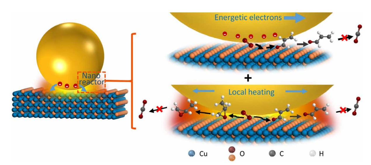
Figure 10. Schematic of the photoelectronic and photothermal contributions to the chemical reaction. Both energetic electrons and local heating effects influence the chemical reaction but through different ways. The energetic electrons regulate the reaction path to improve the acrolein selectivity. The local heating effect of SPs in the hierarchical structure can isolate the active region to eliminate consecutive reactions, thus greatly reducing overoxidation and increasing the selectivity of all partial oxidation products.
(2) Uncovering Photoelectronic and Photothermal Effects in Plasmon Mediated Electrocatalytic CO2 Reduction Remarkably enhanced CO2RR to CO activity and selectivity have been achieved on illuminated Ag NPs electrode by a proper wavelength light over a wide potential window with suppressed HER owing to the LSPR-mediated electrocatalysis. By carefully analyzing the photocurrent (PE and PT) and electrochemical dark current (EC) responses, we quantitatively uncover the PE, PT and EC effects in plasmon-mediated CO2RR to CO and HER. It turns out that the PE effect dominates the former reaction process while the PT and EC effects lead the latter process.
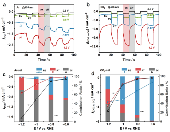
Figure 11. Photocurrent responses of (a) HER and (b) CO2RR to CO on Ag NPs electrode from 0.6 to 1.2 V in (a) Ar-saturated and (b) CO2-saturated 0.1 M KHCO3 upon 405 nm irradiation. The dot lines and the histograms show the current densities of PE, PT and EC as well as the percentages of their contribution to (c) HER and (d) CO2RR to CO currents under illumination at applied potentials in (c) Ar-saturated and (d) CO2-saturated 0.1 M KHCO3. Blue, red, and grey color represent PE, PT, and EC, respectively.
References
1. Zhan Chao*; Yi Jun; Hu Shu; Zhang Xia-Guang; Wu De-Yin; Tian Zhong-Qun*; Plasmon-mediated chemical reactions, Nature Reviews Methods Primers, 2023, 3(12)
2. Wei Ran; Mao Zijie Mao; Jiang Tian-Wen Jiang; Li Hong; Ma Xian-Yin; Zhan Chao*; Cai WenBin*; Uncovering Photoelectronic and Photothermal Effects in Plasmon-Mediated Electrocatalytic CO2 Reduction, Angewandte Chemie International Edition, 2024, e202317740
3. Zhan, Chao#; Wang, Qiu-Xiang#; Yi, Jun; Chen, Liang; Wu, De-Yin; Wang, Ye; Xie, Zhao-Xiong*; Moskovits, Martin*; Tian, Zhong-Qun*; Plasmonic nanoreactors regulating selective oxidation by energetic electrons and nanoconfined thermal fields, Science Advances, 2021, 7(10)
4. Zhan Chao#; Liu Bo-Wen#; Huang Yi-Fan; Hu Shu; Ren Bin*; Moskovits Martin*; Tian Zhong-Qun*; Disentangling charge carrier from photothermal effects in plasmonic metal nanostructures, Nature Communications, 2019, 10(1): 2671-2671
5. Zhan Chao; Wang Zi-Yuan; Zhang Xia-Guang; Chen Xue-Jiao; Huang Yi-Fan; Hu Shu; Li JianFeng; Wu De -Yin*; Moskovits Martin; Tian Zhong-Qun*; Interfacial Construction of Plasmonic Nanostructures for the Utilization of the Plasmon-Excited Electrons and Holes, Journal of the American Chemical Society, 2019, 141(20): 8053-8057
6. Zhan Chao; Chen Xue-Jiao; Yi Jun; Li Jian-Feng; Wu De-Yin; Tian Zhong-Qun*; From plasmonenhanced molecular spectroscopy to plasmon-mediated chemical reactions, Nature Reviews Chemistry, 2018, 2(9): 216-230